Silicon Plasma Wave Receiver for Terahertz Wireless Communication
Extracted from www.epjap.org
This paper presents the design, manufacturing and characterization of an integrated circuit (IC) that uses the plasma oscillations phenomena in silicon nanotransistors (Si-CMOS) for the detection of a 300 GHz-carrier-frequency wireless signal.
We present the strategies for a Si-CMOS-based, wideband, integrated circuit receiver comprising: (i) a physics based, specific plasma-wave-transistor design, allowing impedance matching to the antenna and the amplifier, (ii) a patch antenna engineered through a stacked resonator approach and (iii) a broadband amplifier that uses bandwidth enhancement circuit techniques.
The receiver rectifies a 300 GHz carrier frequency, with a flat and very wideband response, up to10 GHz. This is, to the best of our knowledge, the first demonstration of a low cost 130 nm Si-CMOS technology, plasma wave transistors based, fast and wideband integrated circuit receiver operating at 300 GHz atmospheric window. The results pave the way towards future large scale, and cost effective silicon-technology based, high data bit rate, terahertz wireless communication receivers.
http://www.epjap.org/articles/epjap/pdf/2016/11/ap160302.pdf
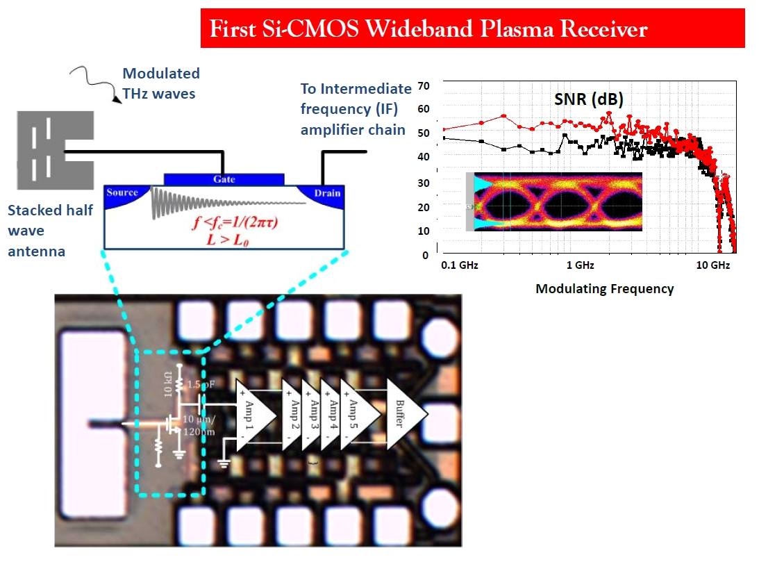
Fig.1 The signal to noise ratio (SNR) of the Si-CMOS receiver versus modulation frequency of the 300GHz carrier.
The inset shows the block diagram with the main components: the patch antenna, the plasma wave FET, with schematically shown damped plasma oscillations, and the integrated wide-band amplifiers chain.
Article posté le 19/12/2016